Direct answer
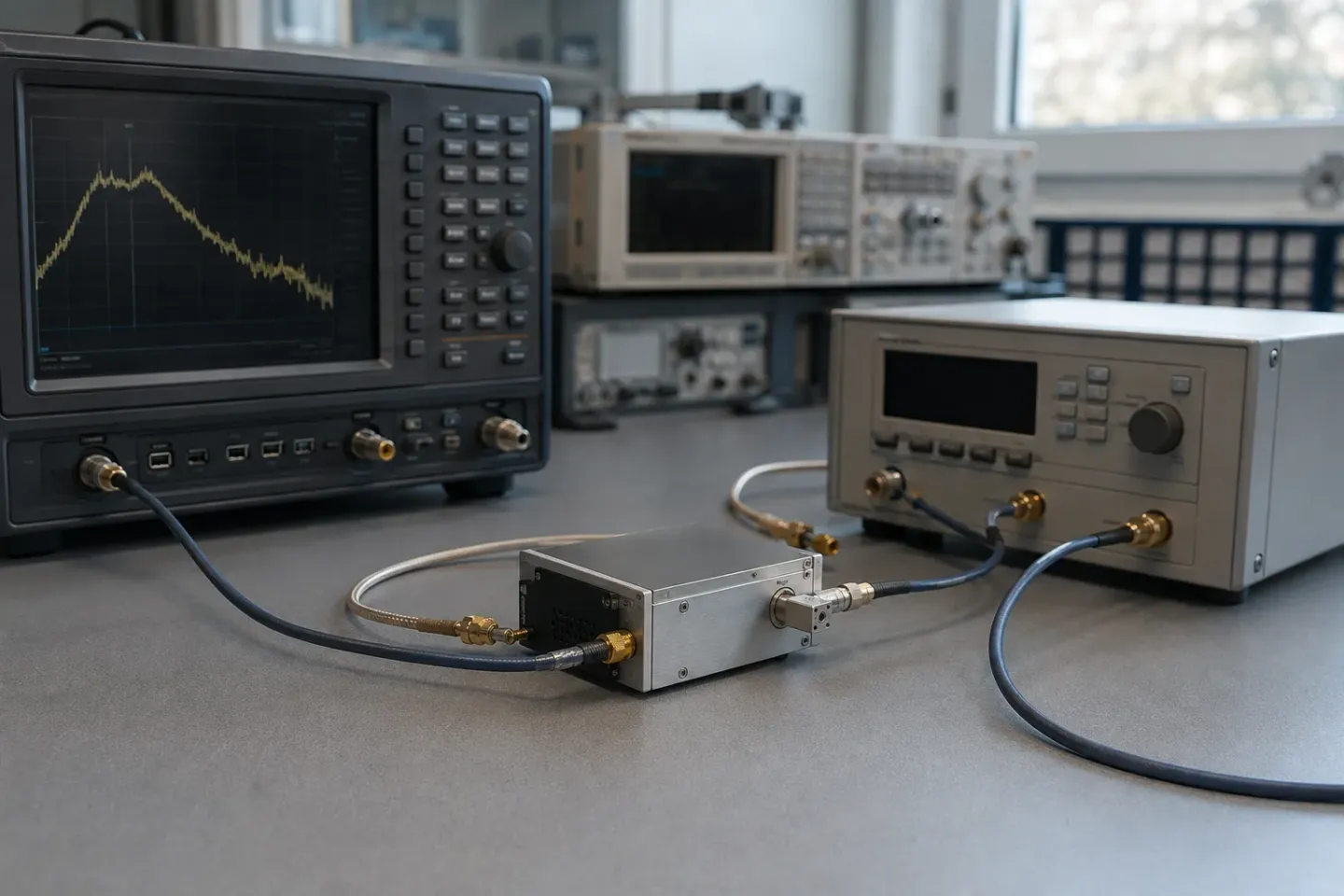
Phase noise describes the short-term random phase fluctuations of an oscillator. The standard measure is single-sideband phase noise, written L(f), defined as the ratio of noise power in a 1 Hz bandwidth at an offset f from the carrier to the total carrier power, expressed in dBc/Hz. Under IEEE 1139, L(f) equals half the spectral density of phase fluctuations, S_φ(f)/2. A phase noise figure is meaningless without both the offset frequency it was measured at and the carrier frequency it was measured on.
Key takeaways
- A single dBc/Hz number is incomplete without its offset and its carrier.
- Which offset matters is set by your system, not by the datasheet.
- Multiplying a carrier by N degrades phase noise by 20·log₁₀(N).
- Jitter is phase noise integrated over a band, so the band has to be stated too.
An ideal oscillator would put all of its power at exactly one frequency. Real ones do not. The energy that ends up either side of the carrier, as random phase fluctuation, is phase noise, and it is usually the parameter that decides whether a source is usable. Of the parameters collected in the engineering guides, it is the one most often quoted and the easiest to compare wrongly.
The definition
The standard measure is single-sideband phase noise, written L(f) and read “script-L of f”. It is the ratio of noise power in a 1 Hz bandwidth, at an offset frequency f from the carrier, to the total carrier power, expressed in dBc/Hz.
Under the IEEE 1139 definition, L(f) = S_φ(f)/2 — half the spectral density of the phase fluctuations. The factor of two is the usual source of confusion when comparing figures from different measurement setups.
Two things follow immediately, and both are practical:
The offset is part of the number. “−110 dBc/Hz” says nothing on its own. −110 dBc/Hz at 1 kHz offset and −110 dBc/Hz at 1 MHz offset describe very different oscillators.
The carrier is part of the number too. Phase noise scales with carrier frequency, so a figure quoted at 1 GHz is not comparable to one quoted at 10 GHz without accounting for it.
Which offset matters is a system question
Datasheets pick offsets that flatter the part. Your system picks the offsets that matter, and they are rarely the same.
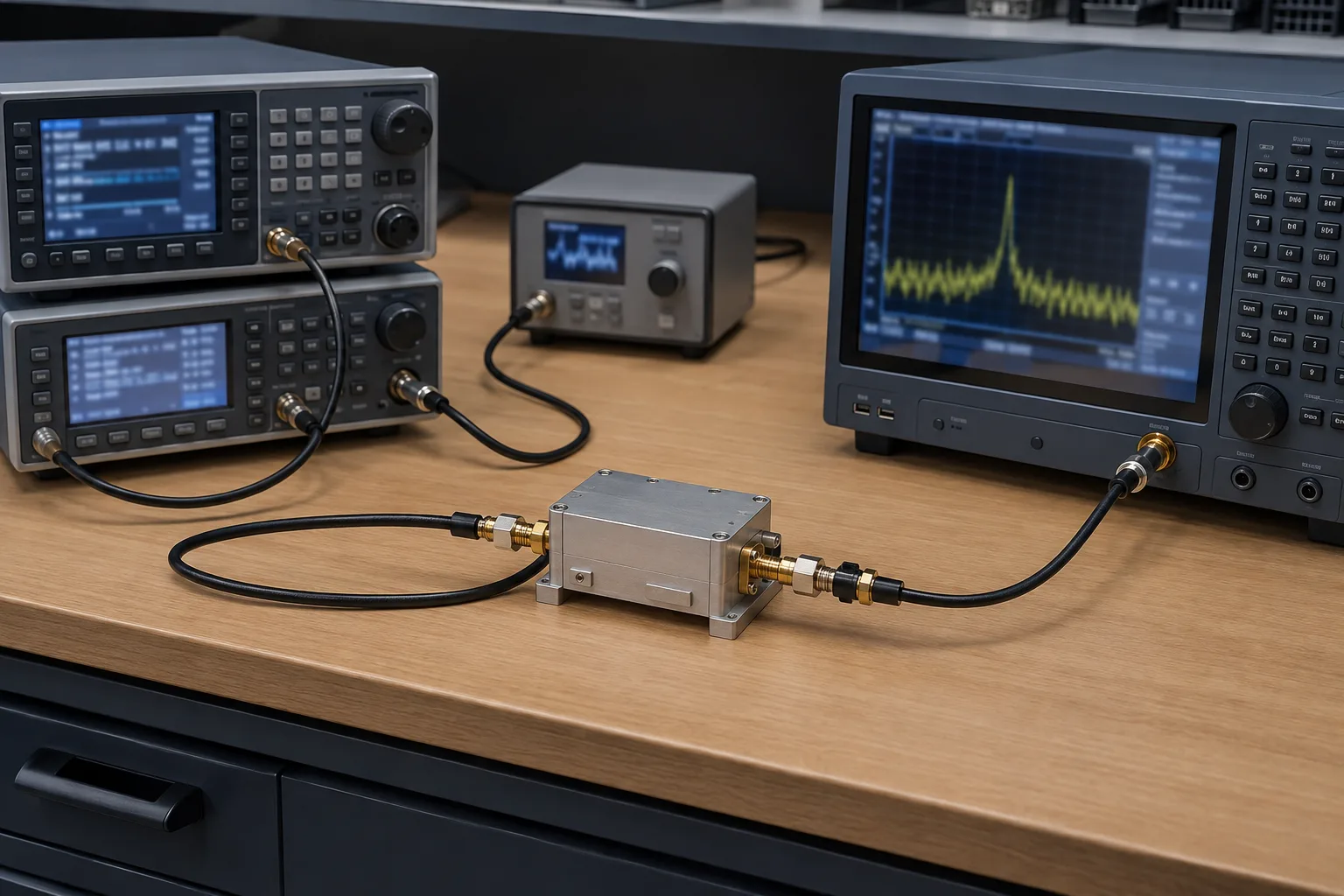
- Close-in (below ~1 kHz). Dominated by flicker processes and by whatever reference the source is locked to. Matters for coherent processing over long dwells, and for anything measuring frequency itself.
- Mid-range (1 kHz to a few hundred kHz). Usually where a phase-locked loop’s own contribution shows up, and where a receiver’s reciprocal mixing against nearby strong signals lives.
- Far-out (beyond the loop bandwidth). Approaches the oscillator’s noise floor. Sets the achievable noise figure of a downconverter, and dominates wideband jitter.
If you cannot say which of those bands your system integrates over, you cannot yet say which source you need.
| Offset band | What lives there | What it constrains |
|---|---|---|
| Below ~1 kHz | Flicker processes, reference noise | Coherent integration over long dwells; frequency measurement |
| 1 kHz – few hundred kHz | Loop contribution, close-in oscillator noise | Receiver reciprocal mixing against nearby strong signals |
| Beyond loop bandwidth | Oscillator noise floor | Downconverter noise figure; wideband RMS jitter |
| Discrete spurs, any offset | Supply, reference and driver artefacts | Spurious responses — these do not integrate like noise |
Band edges are indicative. The boundary that matters in a given design is the loop bandwidth, which you choose.
Reciprocal mixing, concretely
The reason mid-range offsets get so much attention in receiver design is reciprocal mixing. A strong unwanted signal offset by Δf from your wanted one mixes with the LO’s phase noise at that same Δf, and the product lands in the IF as though it were real signal. No amount of IF filtering removes it, because it arrives already inside the passband.
That is also why a YIG-tuned preselector ahead of the mixer buys so much: attenuating the interferer before it reaches the mixer attenuates the reciprocal mixing product with it. The cost is insertion loss, which adds directly to the system noise figure — a trade rather than a free win. The frequency-plan version of that placement is RF, IF and LO.
Multiplication is not free
Phase noise degrades predictably under frequency multiplication. Multiplying a carrier by N multiplies the phase deviation with it, so:
ΔL = 20 · log₁₀(N)
A ×2 doubler costs about 6 dB. A ×8 chain costs about 18 dB, before any noise the multiplier itself adds. This is why generating a clean signal low and multiplying up is often worse than generating it at frequency — and why a wideband fundamental source such as a YIG oscillator can beat a multiplied chain despite looking worse on a headline spec.
Division works the other way, improving phase noise by 20·log₁₀(N), which is why dividing down a clean high-frequency source is a legitimate strategy.
Phase noise and jitter are the same measurement
Jitter is phase noise expressed in the time domain. Converting is an integration, in three steps: convert L(f) from dB to a linear ratio and integrate over the band of interest, double the result to account for both sidebands, then divide by the angular carrier frequency 2πf₀.
For an anchor: a flat −120 dBc/Hz floor on a 1 GHz carrier is approximately 1 ps RMS over the standard 12 kHz to 20 MHz integration band.
The integration limits are not a detail. A jitter figure without its band is as incomplete as a phase noise figure without its offset.
Reading a datasheet plot
- Check the carrier frequency the plot was taken at, and whether it is the one you will run.
- Look for the flat region at high offset — that is the noise floor, and it is often the number that actually constrains you.
- Look for discrete spurs, which are not phase noise and do not integrate the same way. A spur that lands in a critical band matters far more than a decibel of broadband noise.
- Check whether the figure is for the oscillator alone or the locked assembly. They can differ by a lot in the loop-bandwidth region.
What the number does not tell you
Three things routinely surprise people who select on the headline figure alone.
Spurs are not phase noise. A discrete spur is a deterministic tone, not a noise density. It does not integrate the way broadband noise does, and a single spur landing in a critical band can matter more than several decibels of clean noise elsewhere. Datasheets often list them separately, and sometimes not at all.
Locked and unlocked differ inside the loop bandwidth. An oscillator in a PLL takes on the reference’s noise close in and its own noise further out, with the crossover at roughly the loop bandwidth. A figure for the free-running oscillator can be badly misleading about the assembly you will actually ship.
The tuning input is a noise port. Anything that modulates the frequency-control input modulates the output frequency. On a YIG oscillator that is the coil driver; on a VCO it is the tuning voltage. A quiet oscillator behind a noisy control input is not a quiet source.
For how these numbers behave in a magnetically tuned source specifically, see how YIG oscillators work and what YIG is. When the same curve is the thing that decides a source family, see YIG oscillator vs VCO vs DRO. Other parameters that constrain a design in similar ways are collected in the engineering guides section.
Turn a noise plot into a requirement
Begin with the signal that makes the receiver fail, not with a fashionable offset marker. In a receiver, identify the strongest expected unwanted signal, subtract the wanted RF, and use that separation as the first phase-noise offset to inspect. Then ask how much reciprocal-mixing noise can be tolerated in the IF bandwidth. In a transmitter or clock application, identify the integration limits and the permitted RMS phase or time error. The required curve can be uneven: close-in noise may matter for a narrow Doppler bin while far-out noise matters for a wideband modulator.
This method also exposes where a filter helps. A preselector in front of the mixer reduces the unwanted signal that mixes with the LO’s noise; it cannot improve the LO noise density itself. That distinction matters in radar front ends, where a tracking YIG filter and a low-noise LO often appear together but solve different parts of the same blocker problem. If the unwanted signal reaches the mixer through another path, or the offset falls inside the filter passband, the only remaining lever may be the source.
Make the test conditions part of the requirement. Record carrier frequency, output level, tuning or control state, reference source, lock condition, offset range, resolution bandwidth and any excluded spurs. Measure with the final driver and supply arrangement, because the tuning port and reference input can inject noise into a source that looks excellent by itself. For frequency translators, repeat the check through the actual converter plan when the LO is loaded or shared; an isolated source measurement cannot reveal every system spur.
The result should read like an engineering limit rather than a marketing minimum: maximum noise density at named offsets, maximum discrete spur at named offsets, and an integration result over a named band. It gives a future test team a way to decide whether a replacement or repair preserves system performance.
Frequently asked questions
What does dBc/Hz mean?
Decibels relative to the carrier, per hertz of measurement bandwidth. It is a power ratio normalised to a 1 Hz bandwidth so that measurements taken with different resolution bandwidths can be compared.
Is lower always better?
Lower is better at the offsets your system integrates over. Paying for close-in performance you do not use, while ignoring the far-out floor that sets your noise figure, is a common and expensive mistake.
How do phase noise and jitter relate?
RMS jitter is obtained by integrating L(f) over a defined offset band, doubling for both sidebands, and dividing by the angular carrier frequency. The integration limits are part of the answer.
Why does frequency multiplication hurt so much?
Multiplying the carrier multiplies the phase deviation with it, so phase noise degrades by 20·log₁₀(N) for a multiplication factor N. A times-eight multiplier costs about 18 dB before any added noise from the multiplier itself.
Sources
- Phase Noise Measurements with a Real-Time Spectrum Analyzer, chapter 7 — Berkeley Nucleonics Accessed August 28, 2026.
- Accuracy Model for Phase Noise Measurements — NIST Time and Frequency Division Accessed August 28, 2026.
- The Role of the Preselector Filter in a Receiver Front End — RF Essentials Accessed August 28, 2026.